
Long ago in June 2021, famous generation leaker kopite7kimi posted an in depth image of Nvidia’s T234 processor, revealing for the primary time that Nintendo can be receiving a customized variant, dubbed T239. Within the two years that adopted, a wealth of overwhelming proof has necessarily showed that they had been proper. The T239 is a sophisticated cellular processor, in accordance with an octo-core ARM A78C CPU cluster, paired with a customized graphics unit in accordance with Nvidia’s RTX 30-series Ampere structure, mixed with some backported components from the newest Ada Lovelace GPUs – and with an all-new report decompression engine for quick engine. It additionally helps Nvidia’s console-specific graphics API, all however confirming that it is destined for the following technology Transfer.
On this piece, we’re going to communicate in regards to the quite a lot of proof that hyperlinks the T239 with Nintendo and we’re going to even be looking on the closest an identical cellular GPU within the graphics area, downclocking it to ultra-low frequencies in an try to get some more or less deal with on what a low-power Ampere-based graphics core can be offering, whether or not ray tracing is conceivable and simply how vital DLSS upscaling may well be for a 2d technology Nintendo hybrid hand held/console. We’re going to additionally see whether or not our research marries up with any of the sparse data gleaned from the Gamescom appearing of Transfer 2 to choose builders.
However let’s kick off with a elementary, elementary query. Are we able to say evidently, with absolute one hundred pc walk in the park that the T239 is certainly the Transfer 2 chip? That is a damaging. Then again, we will for sure tie the T239 to a Nintendo mission and there is no proof – and certainly, little need – for Nvidia to create this chip for any individual else. For its personal endeavours within the automobile and robotics marketplace, the company already has the T234. And to grasp the customized variant, it is a actually just right thought to get to understand what the T234 is and why Nintendo could not use this chip initially.
This is our video investigation into Nvidia’s T239, its hyperlinks with Nintendo and its doable gaming chronic.
In any case, going again to the primary Transfer, no customized processor was once concerned in any respect. Regardless of advertising from Nvidia to signify differently when the Nintendo hybrid was once introduced, the chip on the centre of the device was once vanilla Tegra X1, albeit with some components (corresponding to its decrease core CPU cores) disabled. Designed from the get-go for the pill, telephone and gaming marketplace, Tegra X1 was once a dud till Nintendo co-opted it for Transfer, the place it discovered a brand new rent of existence. For Transfer 2, Nvidia has not anything within the portions bin that is suitable for a successor. The newest Tegra processors – just like the T234 – are constructed for a completely other, extra tough marketplace. The development blocks are there for an excellent cellular chip, however the present configuration is simply too huge and bloated for a streamlined, mainstream console.
Let’s be transparent right here: the present T234 is a monster of a chip. With a die length of 455mm2, it dwarves the Xbox Collection X processor at 360mm2. It is fabricated the use of the similar Samsung 8nm generation used for the RTX 30-series playing cards, so it is in reality a step in the back of the 7nm and 6nm processes utilized in current-gen consoles. CPU-size, it options 12 ARM A78AE CPU cores, paired with a GPU in accordance with the 30-series Ampere structure with 2048 CUDA cores and a 256-bit reminiscence interface. For the automobile and robotics marketplace, T234 calls for a large number of device studying efficiency, so there may be additionally a deep studying accelerator inbuilt – and its features may also be augmented by means of the tensor cores throughout the GPU.
Nvidia’s T239 – its next-generation gaming processor
What is in an instant transparent is that the T234 is just too giant to paintings in a cellular product. At 455mm2, this processor is far better than the 392mm2 RTX 3070, and with a mix of commonplace sense reasoning, leaks, a large Nvidia Hack and beside the point LinkedIn posts from Nvidia and ex-Nvidia body of workers, we’ve got a just right image of what shape T239 will take. Additionally an important is that Nvidia maintains its personal Linux distribution and whilst a lot of it’s personal, there are sufficient references to T239 in there to get a deal with at the makeup of the processor.
The CPU cluster might be reasonably other than T234’s, for starters. Whilst the A78 ARM cores are common, the AE variant is constructed to satisfy stringent requirements set by means of the Car Electronics Council, with part the cores used to ensure the paintings of the opposite part – utterly beside the point for a video games device. Nvidia’s Linux distribution means that T239 has 8 CPU cores in one cluster, strongly suggesting ARM’s A78C might be used.

Nvidia’s T234 is the foundation for its customized gaming chip for Nintendo – however it needs to be minimize down, just because it is some distance too huge as is for a video games device. On the subject of silicon space, it is 23 p.c better than the chip inside Xbox Collection X.
Nvidia T234
Projected T239
Nvidia RTX 2050 4GB
CPU Structure
12x ARM A78AE
8x ARM A78C
–
GPU Structure
Ampere
Ampere
Ampere
CUDA Cores
2048
1536
2048
Reminiscence/Interface
256-bit/LPDDR5
128-bit/LPDDR5
64-bit/GDDR6
Reminiscence Bandwidth
204GB/s
Max 102GB/s
96GB/s
Reminiscence bandwidth is an important for a cellular gaming device and it is the number one efficiency bottleneck within the recent Transfer. The 256-bit interface in T239 is wildly extravagant for a cellular video games device, and Nvidia’s Linux replace suggests a 128-bit interface, virtually surely paired with LPDDR5 reminiscence. We will have to be expecting absolute most bandwidth of 102GB/s, however in fact, Nintendo can make a selection to downclock that for stepped forward potency. Toughen for DisplayPort – simply configurable for HDMI – is in T239, as it’s in the usual Transfer. The variation here’s that there is sufficient bandwidth for complete HDMI 2.1 toughen, assuming Nintendo makes use of it.
Different spec leaks derived from Nvidia’s Linux distribution are intriguing. There is a complete media encode/decode block on T239 and despite the fact that the chip makes use of RTX 30-series Ampere structure, the media block is backported from the newest Ada Lovelace chips, so it will have to be sooner with toughen for extra codecs, together with AV1. Stepped forward clock-gating – some way of bettering potency from dormant silicon – is some other Ada function that has come what may discovered its method into T239. Energy intake is a bit of of a scorching potato in relation to discussing this chip, for quite a few causes I’m going to take on in a while.
To peer this content material please permit concentrated on cookies.
Organize cookie settings
Nvidia’s Linux distro additionally confirms that T239 has an optical glide accelerator – a core element of DLSS 3 body technology. The issue here’s that it is the final technology Ampere rendition, now not the Ada Lovelace rendition that Nvidia deemed just right sufficient to make frame-gen occur. Whether or not it has a job to play in a possible Transfer successor is still noticed, however it is fascinating that the block was once retained when Nvidia architected this practice, cut-down Tegra.
There is yet another element of T239 worthy of remark – the FDE. It is a completely new {hardware} block now not discovered within the T234. FDE stands for Document Decompression Engine. Very similar to the decompression block present in PlayStation 5, this mainly lets in for ultra-fast decompression of property from garage and into reminiscence. There was once a up to date file from Nate The Hate speaking a few Breath of the Wild demo operating on Transfer 2 {hardware} with 0 loading instances. Neatly, T239 has the {hardware} to facilitate ultra-fast loading, however it’ll want a a lot sooner garage layout to make that conceivable – a space the place we’re missing main points at this time.
The Linux main points paint an overly detailed image of the T239 and lots of of those main points had been showed by means of an Nvidia hack – the Ampere GPU structure, the 128-bit reminiscence bus and LPDDR5 reminiscence, at the side of the backported chronic saving options from the Ada Lovelace design. The hack additionally means that T239 has 1536 CUDA cores, 75 p.c of the cores of the a lot better T234.

Discovered on Wikipedia by means of ‘kopite7kimi’, this die-shot of the Nvidia T234 displays how a lot its space is occupied by means of the CPU and GPU. T239 has 75 p.c of the shaders of the T234, and a way smaller CPU cluster.
We have a chip that is a considerably cutdown Tegra, with redundant options got rid of and a report decompression block added. There are a couple of query marks regardless that. What clock speeds will have to we predict from CPU and GPU? How briskly will the reminiscence run? It is a query that is key to working out efficiency obstacles in a cellular processor. There is additionally the query of whether or not T239 has the deep studying accelerator from the T234 or now not. I consider that is an important to a possible Transfer 2 and its use of DLSS upscaling.
At the clocks query, Nvidia supplies a device for calculating chronic intake at the T234 and it means that the GPU is most productive at 540MHz, a just right candidate for hand held clocks. Potency drops alarmingly the quicker you clock it, and the extra chronic required, the extra warmth is generated. I might be shocked if docked clocks exceeded 1GHz and it generally is a truthful level decrease. 1.0GHz additionally seems like the candy spot for CPU clocks too. Then again, those are calculations for a bigger Tegra chip that is for sure at the 8nm Samsung procedure. A smaller chip may well be extra environment friendly and at this time, there is no proof that confirms completely that it’s nonetheless at the inefficient Samsung 8nm procedure (regardless that I think it’s).
What sort of efficiency will have to we predict from T239?
So, to summarise to this point, now we have were given an in depth thought of the specifications for a chip dubbed T239 that is been in construction for a number of years, which was once first leaked over two years in the past and has since been referenced a number of instances in Nvidia’s Linux distribution and was once discussed within the Nvidia hack and in numerous posts from Nvidia body of workers on LinkedIn. However there may be extra: a smoking gun, if you’re going to. When the unique Transfer was once evolved, Nvidia created a low-level graphics API for buying essentially the most out of the CPU and GPU {hardware}. It was once known as NVM. The Nvidia hack describes an NVN2 graphics API. It means that a number of items of Nvidia {hardware} can be utilized with NVN2 however there are a number of sections of code the place it is specific that it is emulating T239 behaviour on that different {hardware}. In brief, Nvidia has refactored an present Tegra to be smaller, extra environment friendly and supplied with instant loading {hardware} – and it is the use of a next-gen rendition of the Transfer’s NVN graphics API.


The Matrix Awakens demo ran out of VRAM on our downclocked RTX 2050, however Fortnite with {hardware} RT, Nanite and Digital Shadow Maps ran at circa 30fps at 1080p with DLSS efficiency mode. Click on at the thumbnails for upper answer.
So, what will have to be expecting from the T239 in a cellular video games device? Within the contemporary Microsoft FTC courtroom case, Activision’s Bobby Kotick discussed that Nintendo had briefed him at the instrument final yr and its efficiency profile was once consistent with last-gen {hardware}. Neatly, that could be the case however one may similarly say that the Transfer had equivalent horsepower to the Wii U or Xbox 360 however it punched neatly above that weight. This was once accomplished by way of a extra trendy GPU and extra reminiscence, for starters. I might undertaking to signify that Transfer 2 follows that development – and is going additional. I imply, Bobby Kotick talks about PS4-class efficiency, however in the meantime we are listening to communicate of The Matrix Awakens on Unreal Engine 5 operating on it, one thing a PS4 may by no means do. That is what occurs if in case you have customized silicon in accordance with a a lot more trendy GPU, supplied with device studying tensor cores and {hardware} sped up ray tracing.
To get some thought of what a cellular Ampere-class processor can do, I became my hand to a couple sensible paintings. There is no actual an identical counterpart for the features of the A78C CPU cluster within the PC area, however in relation to the GPU, we will get shut. I purchased in a Dell Vostro 5630 comes supplied with the next specifications: a Core i7 1360p CPU, 16 gigs of 4800MHz LPDDR5, a 512GB SSD and an RTX 2050. It is that final element we are shopping at extra intently right here.
To begin with, regardless of its designation as an RTX 20-series section, it is in reality the very same silicon because the Ampere founded RTX 3050 and 3050 Ti – it is a GA107 processor. We will be able to’t fit the 1536 CUDA cores of the T239, however 2048 CUDA cores is the bottom we will move on a gaming Ampere GPU. So why now not merely get a 3050 pc then? Neatly, call to mind the 2050 as a lobotomised 3050 – it has a decrease chronic price range, decrease clocks and crucially, it has got a 64-bit reminiscence interface. At 96GB/s of bandwidth, it operates with a substantial bottleneck in comparison to the RTX 3050 however it additionally provides us ballpark equivalence with the bandwidth a possible Transfer 2 may ship. There is one sticking level regardless that – the 2050 handiest comes with 4GB of RAM. I might be expecting to peer 8GB and even 12GB of general device reminiscence in Transfer 2.

A hushed awe please for the extremely mediocre Dell Vostro 5640. A Core i7 1360p CPU drives the {hardware}, however it is the RTX 2050 4GB GPU we are serious about – the bottom acting Ampere-based cellular GPU lets to find. We downclocked it from circa 1350MHz to only 750MHz for our gameplay checks.
You’ll be able to see the result of my checks within the video atop this web page, however sooner than we move on, let’s be transparent: that is the nearest approximation we will get in combination for the T239 GPU, however extra as it should be, what you might be seeing within the video is an extremely low-spec Ampere GPU operating at meagre clock speeds, starved of reminiscence bandwidth. It will possibly handiest actually give us a ballpark thought of what a cellular Ampere chip can ship, even if I downclocked it to a ridiculously low 750MHz – besides, the consequences are intriguing.
I could not get The Matrix Awakens operating owing to the 4GB reminiscence limitation at the RTX 2050 and it kind of feels that the demo calls for round 5.6GB on the minimal. Then again, the absolutely enabled Fortnite UE5 enjoy the use of Lumen, Nanite and Digital Shadow Maps does paintings. Certainly, in contrast to the console variations, we do in reality have get entry to to {hardware} sped up ray tracing within the PC model and sure, it does run at the RTX 2050 pc. I examined {hardware} RT Lumen, its instrument variant, and I additionally examined at local 720p and a number of other DLSS variants, all resolving to a 1080p output. For the report, instrument RT with DLSS efficiency mode (540p in, 1080p out) is the winner however between easiest and worst effects right here, there may be only a 9.5 p.c distinction, and in fps phrases that is simply 2.82fps.
My bet is that the Matrix Awakens demo for Transfer 2 founded on the right track {hardware} almost definitely is actual, however Epic should be doing a large number of paintings in making Unreal Engine 5’s key options run neatly at the new Nintendo device, just because The Matrix Awakens is so much heavier at the GPU than Fortnite. That being the case, simply operating PC code on a low chronic Ampere GPU is not prone to be that revealing. Nonetheless, it does run. You’ll be able to use {hardware} RT. DLSS is useful.


Starved of reminiscence bandwidth, CUDA cores and clock velocity, the RTX 2050 by way of DLSS can nonetheless ship convincing 1080p gameplay for Keep an eye on (with RT reflections), Cyberpunk 2077, A Plague Story: Requiem and Dying Stranding. Relating to the latter, we will even run at 1440p output at 30fps with DLSS efficiency mode.
I additionally attempted Dying Stranding, benchmarking its GPU-heavy intro. At 1080p local, the collection averages at 34.9fps, which does toughen the last-gen horsepower narrative. At 720p, frame-rate rises to 52.5fps. I have additionally run this bench at DLSS high quality mode too – 67 p.c of local res. 34.9fps moderate will increase to 44.7fps. At 720p with DLSS, frame-rate does build up however the efficiency differential is tricky to as it should be measure for the reason that collection is in reality capped at 60fps. Nonetheless, shopping at gameplay, 1440p in DLSS efficiency mode is viable in this little Ampere-based GPU and whilst a lot of the sport performed out locked at 30 frames according to 2d, there have been some dips underneath. In a war of words with the BTs, the heavy post-processing gave the look to be an excessive amount of for the GPU to deal with.
DLSS toughen: helpful for Transfer 2 or completely an important?
I consider that DLSS is an important to the following Nintendo device, however whether or not we’re going to get the fabled ‘Transfer 4K’ comes down as to whether a core element of the unique T234 has made its method into T239. I am regarding the Deep Finding out Accelerator – a separate {hardware} block that may mix its personal processing with the tensor cores throughout the GPU. My checks with the RTX 2050 counsel that DLSS may well be helpful for upscaling to 1080p and even perhaps 1440p, as we noticed in Dying Stranding. Then again, the upper the output answer, the upper the price of DLSS. In Dying Stranding, the extra price of upscaling 720p to 4K (DLSS extremely efficiency mode) is over 18ms. For a 60fps demo, simply the processing price of DLSS exceeds the 16.7ms render time for the entire body. Then again, if the DLA has made its method from T234 to T239, DLSS can have some distance much less of a computational price.
Additionally it is vital to worry how vital DLSS is to the entire Transfer 2 endeavor. As you can see within the video, all of our gameplay checks produced some fairly spectacular effects – however all required the usage of DLSS, upscaling from quite a lot of inner resolutions to 1080p. So, within the PC area, it is in most cases thought to be that it is ‘OK’ to run the upscaler at efficiency mode at 4K, balanced mode at 1440p and high quality mode at 1080p. Console gaming in the lounge is other, you might be sat a lot additional clear of the display and symbol high quality expectancies are other. In any case, now we have noticed some remarkably low answer already this technology, even from PS5 and Collection X.
So, I in reality assume for a cellular chipset connected to a front room show, 1080p efficiency mode upscaling from a local 540p will glance appropriate, whilst 1080p from local 720p (DLSS high quality mode) seems lovely nice. It is going to surely glance significantly better than lots of the tough Transfer video games now we have noticed in docked play. DLSS 4K extremely efficiency mode upscaling from a local 720p? Once more, test it out within the video above – it is some distance from a pristine 4K, however a low-power console does not wish to mimic local 4K. It simply wishes to supply a tight symbol on a 4K front room TV.
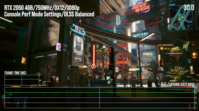

This is how our ultra-low spec Ampere GPU copes with Cyberpunk 2077 2.0 tuned to PS5’s efficiency mode settings with DLSS at 1080p balanced mode. Necessarily, we are shopping at 25fps to 30fps. Pass judgement on the picture high quality your self by means of clicking at the thumbnails.
And that’s the reason mainly the place I am as much as at this time with Transfer 2, its technological makeup and the type of ballpark efficiency that an ultra-pared again Ampere GPU can ship. There may be nonetheless controversy and lots of unresolved questions. There are some who consider that the T239 was once meant for a scrapped ‘Transfer 4K’ or ‘Transfer Professional’ and that the true subsequent technology Transfer will be offering one thing other. I do not accept as true with this: the extent of funding required to make T239 and the scale of the GPU at the side of its customized blocks represents a right kind, subsequent technology bounce over the Tegra X1.
Questions and considerations: is T239 viable for a hand held?
Then again, there are some extra professional questions and considerations over the T239. We’ve got established that the 455mm2 T234 is far, method too huge for a cellular video games processor – however even with its quite a lot of cutbacks in CPU and graphics, the T239 might be a lot better than the 118mm2 Tegra X1 within the recent Transfer. A bigger chip calls for meatier cooling which might not be a just right fit for a Nintendo hybrid hand held/house console. Some consider that T239 is not at the 8nm Samsung procedure node in any respect, and it is most probably that just a teardown of the retail device will ascertain this a technique or some other.
From my point of view, the secret is that by means of a means of removal, T239 is the most efficient candidate for the processor on the middle of the brand new Nintendo device. Nvidia’s Jensen Huang is at the report as pronouncing that Nvidia’s partnership with Nintendo will most probably final twenty years. And with a mooted 2024 unencumber date, there were no convincing leaks in anyway for another processor that would to find its method into the brand new Transfer.

The DLSS conundrum. All readings listed below are derived from local 720p, then DLSS upscaling is added to hit 1080p, 1440p and 2160p resolutions. DLSS is not a ‘unfastened lunch’ and the Tensor cores within the GPU on my own can handiest do such a lot. Then again, if T239 contains T234’s Deep Finding out Accelerator, that would vastly cut back DLSS’s overhead.
I had a good time striking in combination the ones sensible checks with the RTX 2050 and it will give you some thought of what the lowliest Ampere-based GPU can be offering. Any trendy sport turns out to run simply nice on it, assuming you modify settings accordingly. And DLSS is – as soon as once more – a game-changer and doubtlessly much more transformative if the Deep Finding out Accelerator block is in there.
However simply let me rigidity yet another time that that is handiest the nearest approximation we will make to the mooted T239 spec: whilst clocks are low, CUDA cores are upper. Whilst reminiscence bandwidth is paltry in PC phrases, it is ballpark with the most efficient that T239 may be offering – and Nintendo would possibly make a selection to downclock. And naturally, in our checks, there is no competition on that bandwidth from the CPU – some other doable drain on efficiency.
Even so, there may be promise right here – and keep in mind that I’m the use of PC variations of the video games I examined, and not using a scope for customisation for a cellular platform. And actually, the magic goes to return from the builders themselves. Have a look again at when Doom 2016 first seemed on Transfer, or The Witcher 3, or the Crysis remasters, or the fantastic ports produced by means of Riot North just like the Sniper Elite and Zombie Military video games. Those video games defied the technological limits of the Tegra X1 and without reference to the T239’s specifications, I be expecting to peer the similar subsequent time round too.

Recreation Rant not too long ago reported on a brand new Nintendo patent for a device with twin monitors that may perform independently. Whether or not that is anything else to do with the brand new Transfer is still noticed however it does lift a captivating level: we all know extra in regards to the inner {hardware} of the device than we do about the idea that of the instrument itself?
Transfer 2: the large questions we haven’t any solutions for
A few of our exceptional questions across the subsequent technology Transfer will most probably get some solutions when we see the {hardware}. How giant is it? What sort of battery existence is being promised? What’s going to the video games appear to be? To what extent can present Transfer {hardware} – together with its JoyCons – paintings with its successor? We might also get some additional disclosure from Nvidia itself at the position it has performed within the construction of the device.
In accordance with the whole lot I have discovered about T239 over the months, I believe my greatest wonder is how bold the {hardware} is. Given the risk to re-architect a brand new, games-centric processor, Nvidia can have adopted the direction it laid down with its GTX 16-series graphics playing cards by means of stripping out device studying and RT {hardware}, or paring them again to the minimal with cut-price choices (like the best way AMD built-in {hardware} RT into RDNA 2 with an emphasis at the lowest silicon price conceivable). As a substitute, the proof means that Nvidia and Nintendo have agreed on a design that arguably over-delivers on next-gen options, whilst the Document Decompression Engine (FDE) issues to high quality of existence additions to the silicon {that a} firmly oriented round an excellent gaming enjoy. May just this be essentially the most forward-looking {hardware} design from Nintendo for the reason that GameCube?
And whilst questions stay round the use of Samsung 8nm silicon, there’s a silver lining for Nintendoin handing over a revised style additional down the road. It would embody 6nm, 5nm or 4nm applied sciences for stepped forward thermals and battery existence, simply because it did with the revised Transfer, the OLED style and Transfer Lite. Within the brief time period, the query is how huge T239 might be and if its traits imply we want a bigger hand held – one thing I do not believe Nintendo would need.
At the moment, the quite a lot of leaks and unofficial disclosures imply that we most probably know way more in regards to the internals of the following Nintendo device than we do about different extra vital components – like the entire thought of the brand new {hardware}, as an example. T239 is a mobile-orientated processor, whilst Nintendo’s centralisation of all construction assets to 1 platform signifies that we are virtually surely shopping at some other Transfer, as antagonistic to a couple more or less logo new thought. Then again, with Nintendo’s historical past, a instantly Transfer 2 turns out virtually too easy – however with preliminary disclosure with a bit of luck now not too some distance away, with a bit of luck we’re going to have a greater point of view at the new device quickly.
To peer this content material please permit concentrated on cookies.
Organize cookie settings


 – Underbaked Motion-RPG Fare That Performs Tough On Transfer")


